Technology
We design, advise and deliver multiple technology options for customers.
Our PCB Portfolio gives you an overview of some of the important features of each technology.
We welcome customer discussions, so get in touch and one of our experts will guide you through the technology solution that best meets your needs.
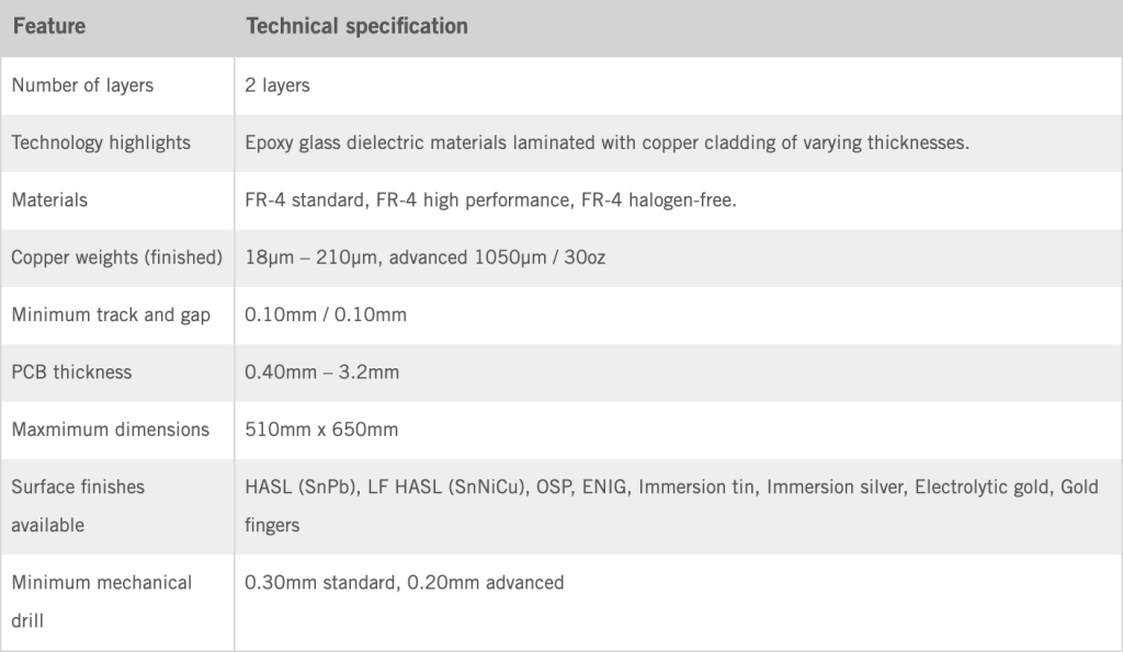
Double sided PCBs
Our product portfolio includes double sided PCBs for a wide range of applications from medical to industrial controls. This segment is decreasing as our customer’s demands for high layer count boards increases. However, we still produce large volumes with the same quality standards and expectations as our more advanced boards.
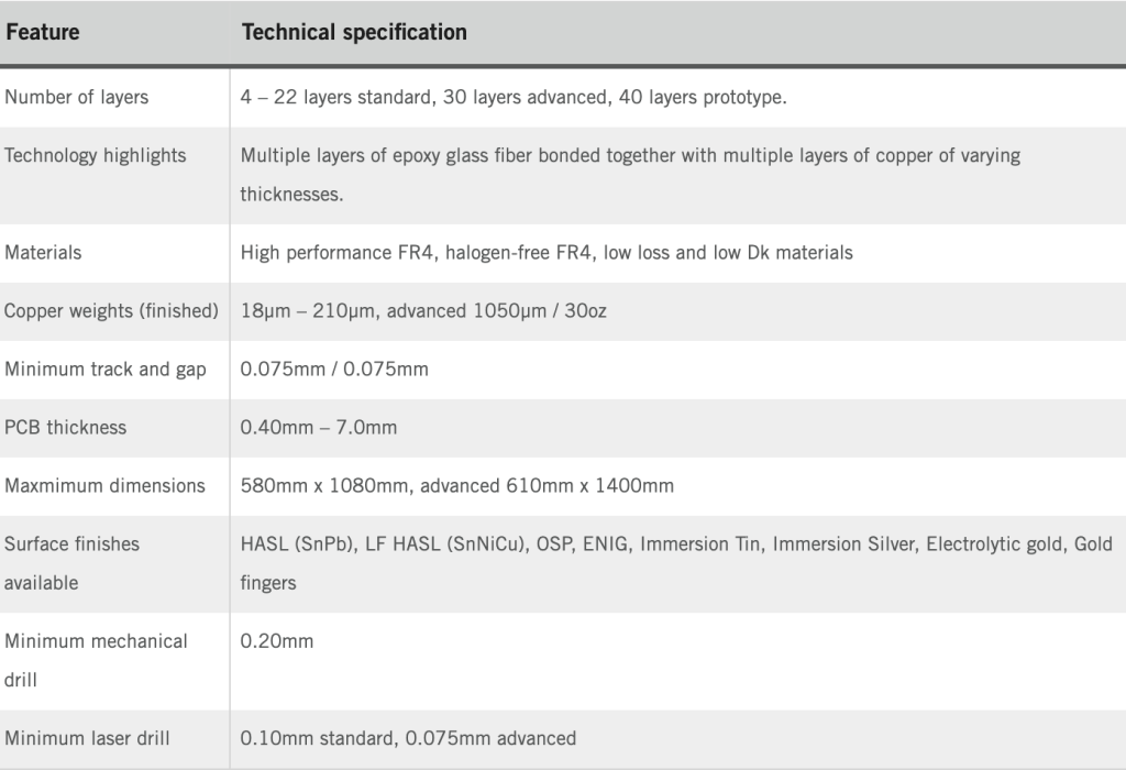
Multilayer PCBs
It is a PCB made with three or more conductive copper layers. The conductive foil appears to be various layers of a multi-sided circuit board. The different inner layers are processed in pairs (on a core) and then bonded together using prepreg as the insulating layer. The layers are then placed in such a way that both sides of the PCB can be used to mount components with additional tracking/electrical connections on the inside of the board. Vias are used as a source of the electrical connections between the different layers of a multilayer PCB.
Many products use multilayer PCBs, including computers, medical equipment, in-car systems, GPS and satellite systems, industrial control systems
Many products use multilayer PCBs, including computers, medical equipment, in-car systems, GPS and satellite systems, industrial control systems
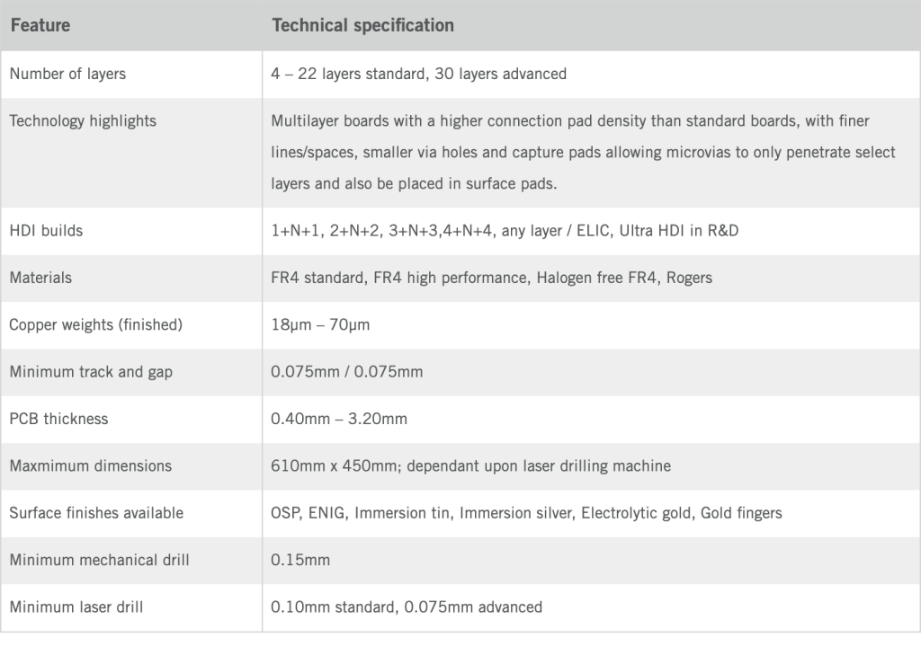
HDI – High Density Interconnect PCBs
From 1+N+1 to X+N+X stack-ups, “all layer” technology and in a wide range of technological variants.
An HDI PCB is a PCB which has a far higher wiring density than a conventional through hole PCB. Per IPC-6012 (1.4.1) this is defined as a design which has an average number of electrical connections/cm² of 20 or more, on both sides of the PCB.
An HDI PCB uses finer features than a conventional PCB, enabling tighter packaging densities and lower layer count and/or reduced size. All HDI PCBs should follow IPC2226 – Sectional Design Standard for High Density Interconnect (HDI) Printed Boards. IPC2226 separates HDI into types I to type VI depending on usage and complexity.
Typical applications are smartphones, where space is at a premium, and aerospace where smaller size and/or reduced weight are key drivers.
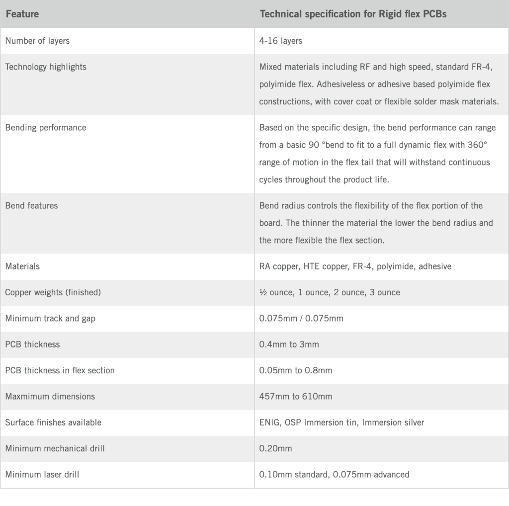
Rigid-flex PCBs
As the name implies, a Rigid-Flex PCB is a hybrid of a Flex PCB and a Rigid PCB. The combination of the two types of boards utilises the benefits each one provides, integrating the versatility of the flexible board with the robustness of the rigid board. Rigid-flex printed circuit boards are used in more complex mechanical designs, eliminating flexible cables and wiring and replacing it with integrated circuits.
Rigid-Flex PCBs, by definition, are a combination of rigid part(s) joined by interconnecting flex areas where the flex material is used across the entire PCB area.
The rigid parts are where there is no bending requirement. Again, PTHs take connections from layer to layer as required. Rigid-flex may also employ other technologies as required eg. HDI. Unlike the cost-effective flex PCBs, Rigid-Flex PCBs can be a bit more costly due to their intricate design.
Rigid-flex PCB design can be used to eliminate or greatly reduce requirements for bulky and costly cable harnesses, in turn taking out costs and reducing assembly time. Like the pure flexible PCBs, a high volume of rigid-flex PCBs are used in aviation and space applications – and also in automotive and test equipment.